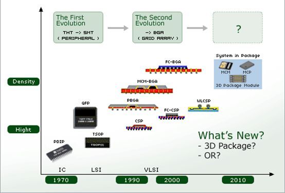
1.Packaging development history
For packaging, from low-level to high-level, it is a chip (IC) + shell (Package).
Due to process limitations, the early design was that after the chip was packaged, it was connected to the circuit board through pins.
In the 1990s, with the advancement of technology and consumer demand, BGA was born.
The biggest improvement is that the pin connections around the package are improved to solder ball connections at the bottom of the package, which greatly improves the utilization of the area.
2.
After the 1990s, the structure is basically the same. CSP, WLP, etc. further reduce the pin size and improve the assembly density.
The package of 2D IC developed to the extreme is shown in the figure, and the ratio of chip area to package area has reached the limit.
Since the subtitles are spoilers for 2D, there is naturally a 3D IC. Although the IC stacking method in this picture has begun to use space, it still does not appear to be very advanced.
After all, only chips of the same function can be stacked here, and there are various connections flying around.
3.Elementary3D IC SIP
The interposer silicon layer is used as a passive element;
4.complete model
Note: Don't look at these pictures as thick as a hamburger. In fact, the thickness of the interposer is generally only 0.2mm-0.7mm, and the entire package is actually very, very, very small.